Samsung Electronics showcases its new automotive technology strategy at Foundry Forum EU 2023
Since the development and mass production of the world's first eMRAM based on 28nm FD-SOI in 2019, Samsung Electronics has been promoting the development of AEC-Q100 level 1 applications based on 14nm FinFET.
Samsung Electronics provided advanced and comprehensive process solutions for the automotive industry at the Foundry Forum EU 2023 held in Munich on October 19th, covering from the most advanced 2-nanometer process to 8-inch traditional processes.
In order to meet the latest innovative needs of the automotive market, Samsung will develop the industry's first 5-nanometer eMRAM solution for future automotive technology. EMRAM is the next generation memory for automotive applications, which can achieve high read and write speeds and excellent thermal stability.
Since the development and mass production of the world's first eMRAM based on 28nm FD-SOI in 2019, Samsung Electronics has been promoting the development of AEC-Q100 level 1 applications based on 14nm FinFET. Samsung OEM plans to expand its product portfolio to 14 nanometers by 2024, 8 nanometers by 2026, and 5 nanometers by 2027.
Compared to the previous 14 nanometer technology, the Samsung 8 nanometer eMRAM solution has a 30% increase in density and a 33% increase in speed.
From Innovation to Traditional Automotive Process Solutions
The company has released its advanced process roadmap and emphasized its plan to achieve mass production capacity of 2nm technology for automotive applications by 2026. Samsung Electronics has also strengthened its commitment to meeting customer needs by expanding its 8-inch BCD (bipolar CMOS DMOS) process portfolio.
The BCD process combines the advantages of three different process technologies on a single chip: bipolar (B), CMOS (C), and DMOS (D), and is most commonly used in the manufacturing of power semiconductors. Samsung Electronics plans to expand its current 130nm automotive BCD product portfolio to 90nm by 2025. The 90nm BCD process is expected to reduce the chip area by 20% compared to the 130nm process.
By adopting deep trench isolation (DTI) technology to shorten the distance between each transistor and improve power density, Samsung's foundry will be able to operate at voltages up to 120V instead of just 70V, thereby expanding its wide range of possible applications. This will enable the company to provide a Process Development Kit (PDK) capable of supporting up to 120V 130nm BCD processes by 2025.
Innovating beyond Moore through the Advanced Packaging Alliance
Samsung collaborated with its SAFE partners and major players in the fields of memory, packaging substrates, and testing to complete the creation of the Multi Chip Integration (MDI) alliance.
As part of an industry wide partnership of 20 partners, Samsung is a leader in developing 2.5D and 3D packaging solutions tailored for all applications from automobiles to high-performance computing (HPC).
What are the latest developments in SiC and GaN 'boarding'?
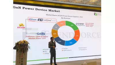
Although SiC has been widely used in automobiles, the cost of SiC devices is still too high for most cars due to yield and cost-effectiveness issues; The commercial use of GaN is concentrated in the f…What are domestic chip manufacturers doing with the rapid landing of large models?
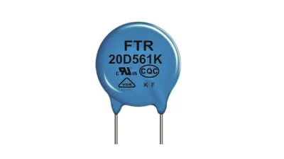
The turning point for 2022-2023 has arrivedWhat is the turning point for 2022-2023? It is the emergence of the AI big model that has turned the marginal cost of acquiring knowledge into a fixed cost. …FTR20D681K Varistor Applications and Technical Advantages: Providing Comprehensive Protection for Your Circuits
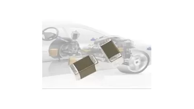
Product Overview:In modern electronic design, overvoltage protection has become a crucial element in ensuring the stability and reliability of circuits and devices. The FTR20D681K varistor is a high-p…HRE CAA/CAI Series Automotive Grade MLCC Capacitor Selection Guide
HRE CAA/CAI Series Automotive Grade MLCC Capacitor Selection GuideWith the rapid advancement of automotive electronics, high-performance and high-reliability MLCC capacitors have become critical for t…
- Top News
- HRE CSA Series Commercial Grade MLCC Capacitor Selection Guide
- HRE CIA Series Industrial Grade MLCC Capacitor Selection Guide
- HRE CAA/CAI Series Automotive Grade MLCC Capacitor Selection Guide
- FTR20D681K Varistor Applications and Technical Advantages: Providing Comprehensive Protection for Your Circuits
- Samsung Electronics showcases its new automotive technology strategy at Foundry Forum EU 2023


